Jawbreaker
HackRF Jawbreaker is the beta test hardware platform for the HackRF project.
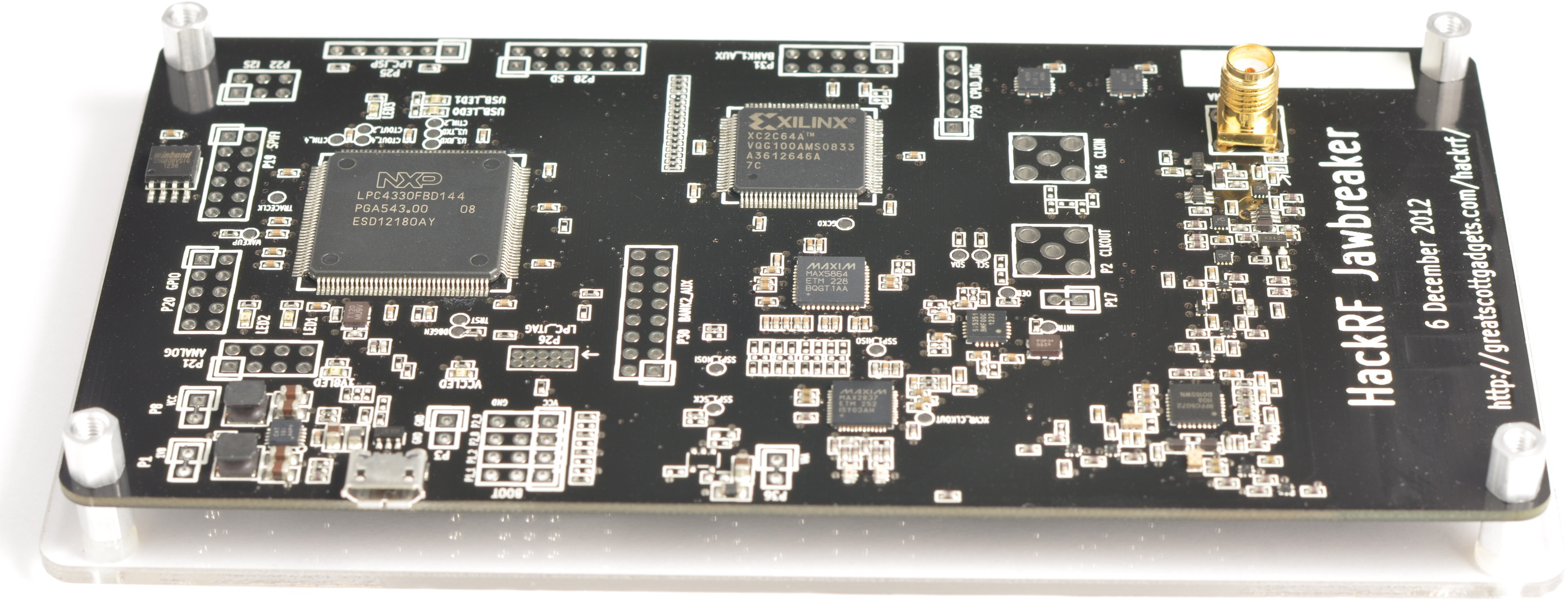
(Jawbreaker picture provided by fd0 with Creative Commons License CC BY 3.0.)
Features
half-duplex transceiver
operating freq: 30 MHz to 6 GHz
supported sample rates: 8 Msps to 20 Msps (quadrature)
resolution: 8 bits
interface: High Speed USB (with USB Micro-B connector)
power supply: USB bus power
portable
open source
Hardware Documentation
Schematic diagram, assembly diagram, and bill of materials can be found at https://github.com/greatscottgadgets/hackrf/tree/master/hardware
Transmit Power
The maximum TX power for Jawbreaker varies by operating frequency:
30 MHz to 100 MHz: 5 dBm to 15 dBm, increasing as frequency decreases
100 MHz to 2300 MHz: 0 dBm to 10 dBm, increasing as frequency decreases
2170 MHz to 2740 MHz: 10 dBm to 15 dBm
2700 MHz to 4000 MHz: -5 dBm to 5 dBm, increasing as frequency decreases
4000 MHz to 6000 MHz: -15 dBm to 0 dBm, increasing as frequency decreases
Overall, the output power is enough to perform over-the-air experiments at close range or to drive an external amplifier. If you connect an external amplifier, you should also use an external bandpass filter for your operating frequency.
Before you transmit, know the laws for the region you are transmitting in. Jawbreaker has not been tested for compliance with regulations governing transmission of radio signals. You are responsible for using your Jawbreaker legally.
SMA, not RP-SMA
The connectors on Jawbreaker are SMA, not RP-SMA. SMA connectors and RP-SMA connectors look extremely similar, the difference is that SMA connectors have a center pin. RP-SMA connectors are common on 2.4 GHz antennas and are popular on Wi-Fi equipment. If you connect an RP-SMA antenna to Jawbreaker, it will seem to connect snugly but won’t function at all because neither the male nor female side has a center pin.
Recommended PCB and Antenna Changes
Jawbreaker has an SMA antenna connector and it also includes a built-in PCB antenna intended for operation near 900 MHz. The built-in PCB antenna isn’t a very good antenna. A paperclip stuck into the SMA connector of the Jawbreaker is likely to be better. We recommend that you free your Jawbreaker to operate with better antennas by cutting the PCB trace to the PCB antenna with a knife. This enables the SMA connector to be used without interference from the PCB antenna.
The trace to be cut is between the two solder pads inside a box labeled R44. There is an arrow printed on the board that points to the R44 box. A video that demonstrates the antenna modification is on YouTube: HackRF Antenna Modification.
Due to a manufacturing error, there is solder on the pads in box R44 that you should try to remove before you cut the trace. R44 may appear as a single solder blob. If you have a soldering iron and solder wick/braid, use a soldering iron and fine solder wick to remove as much solder as you can from the two R44 pads. Then, use a pen knife to gently cut away the area between the two R44 pads. Make multiple, gentle cuts, instead of one or two forceful cuts. As you cut, you’ll break through the black solder mask, then the copper trace between the pads, and stop when you reach fiberglass. Remove the copper trace completely, so just the two R44 pads remain. Use a multimeter or continuity tester to verify that the two R44 pads are no longer connected. If you don’t have a soldering iron, you can cut through the copper trace and the solder blob all at once, but it requires a bit more effort. The only reason not to cut the PCB trace is if you want to try Jawbreaker but don’t have any antenna with an SMA connector (or adapter).
If you want to restore the PCB antenna for some reason, you can install a 10 nF capacitor or a 0 ohm resistor on the R44 pads or you may be able to simply create a solder bridge.
Expansion Interface
LPC
Boot config
Default boot configuration is SPIFI. Install headers and jumpers (and optionally resistors) to reconfigure.
Pin |
P43 |
P32 |
P42 |
P27 |
|---|---|---|---|---|
1 |
VCC |
VCC |
VCC |
VCC |
2 |
P2_9 |
P2_8 |
P1_2 |
P1_1 |
3 |
GND |
GND |
GND |
GND |
The table below shows which pins to short per header for a given selection.
Selection |
P43 |
P32 |
P42 |
P27 |
|---|---|---|---|---|
USART0 |
2-3 |
2-3 |
2-3 |
2-3 |
SPIFI |
2-3 |
2-3 |
2-3 |
1-2 |
USB0 |
2-3 |
1-2 |
2-3 |
1-2 |
USSP0 |
2-3 |
1-2 |
1-2 |
1-2 |
USART3 |
1-2 |
2-3 |
2-3 |
2-3 |
P19 SPIFI Intercept header
Traces may be cut to install header and jumpers or use off-board SPI flash.
Pin |
Function |
|---|---|
1 |
Flash DO |
2 |
SPIFI_MISO |
3 |
Flash DI |
4 |
SPIFI_MOSI |
5 |
Flash CLK |
6 |
SPIFI_SCK |
7 |
Flash CS |
8 |
SPIFI_CS |
9 |
Flash Hold |
10 |
SPIFI_SIO3 |
11 |
Flash WP |
12 |
SPIFI_SIO2 |
P20 GPIO
Pin |
Function |
|---|---|
1 |
GPIO3_8 |
2 |
GPIO3_9 |
3 |
GPIO3_10 |
4 |
GPIO3_11 |
5 |
GPIO3_12 |
6 |
GPIO3_13 |
7 |
GPIO3_14 |
8 |
GPIO3_15 |
9 |
GND |
10 |
GND |
P21 Analog
Pin |
Function |
|---|---|
1 |
GND |
2 |
ADC0_6 |
3 |
GND |
4 |
ADC0_2 |
5 |
GND |
6 |
ADC0_5 |
7 |
GND |
8 |
ADC0_0 |
P22 I2S
Pin |
Function |
|---|---|
1 |
VCC |
2 |
I2S0_TX_SDA |
3 |
I2S0_TX_WS |
4 |
I2S0_TX_SCK |
5 |
I2S0_TX_MCLK |
6 |
GND |
P25 LPC_ISP
Pin |
Function |
|---|---|
1 |
GND |
2 |
ISP |
3 |
NC |
4 |
U0_RXD |
5 |
U0_TXD |
6 |
RESET |
P26 LPC_JTAG
Pin |
Function |
|---|---|
1 |
VCC |
2 |
TMS |
3 |
GND |
4 |
TCK |
5 |
GND |
6 |
TDO |
7 |
NC |
8 |
TDI |
9 |
GND |
10 |
RESET |
P28 SD
Pin |
Function |
|---|---|
1 |
GND |
2 |
VCC |
3 |
SD_CD |
4 |
SD_DAT3 |
5 |
SD_DAT2 |
6 |
SD_DAT1 |
7 |
SD_DAT0 |
8 |
SD_VOLT0 |
9 |
SD_CMD |
10 |
SD_POW |
11 |
SD_CLK |
12 |
NC |
CPLD
P29 CPLD_JTAG
Pin |
Function |
|---|---|
1 |
CPLD_TMS |
2 |
CPLD_TDI |
3 |
CPLD_TDO |
4 |
CPLD_TCK |
5 |
GND |
6 |
NCC |
P30 BANK2_AUX
Pin |
Function |
|---|---|
1 |
B2AUX1 |
2 |
B2AUX2 |
3 |
B2AUX3 |
4 |
B2AUX4 |
5 |
B2AUX5 |
6 |
B2AUX6 |
7 |
B2AUX7 |
8 |
B2AUX8 |
9 |
B2AUX9 |
10 |
B2AUX10 |
11 |
B2AUX11 |
12 |
B2AUX12 |
13 |
B2AUX13 |
14 |
B2AUX14 |
15 |
B2AUX15 |
16 |
B2AUX16 |
P31 BANK1_AUX
Pin |
Function |
|---|---|
1 |
B1AUX9 |
2 |
B1AUX10 |
3 |
B1AUX11 |
4 |
B1AUX12 |
5 |
B1AUX13 |
6 |
B1AUX14 |
7 |
B1AUX15 |
8 |
B1AUX16 |
9 |
GND |
10 |
GND |
External clock
P2 CLKOUT
Install C165 and R92 as necessary to match output. For CMOS output, install 0 ohm resistor in place of C165; do not install R92.
Pin |
Function |
|---|---|
1 |
CLKOUT |
2 |
GND |
3 |
GND |
4 |
GND |
5 |
GND |
P16 CLKIN
Install C118, C164, R45, R84 and R85 as necessary to match input.
For CMOS input, install 0 ohm resistors in place of C118 and C164; do not install R45, R84, or R85.
Pin |
Function |
|---|---|
1 |
CLKIN |
2 |
GND |
3 |
GND |
4 |
GND |
5 |
GND |
P17 CLKIN_JMP
Cut P17 short (trace) to enable external clock input. If short is cut, a jumper should be used on P17 at all times when an external clock is not connected to P16.
Pin |
Function |
|---|---|
1 |
GND |
2 |
CLKIN |
More
Additional headers are available. See the board files for additional details.
Differences between Jawbreaker and HackRF One
Jawbreaker was the beta platform that preceded HackRF One. HackRF One incorporates the following changes and enhancements (at minimum):
Antenna port: No modification is necessary to use the SMA antenna port on HackRF One.
PCB antenna: Removed.
Size: HackRF One is smaller at 120 mm x 75 mm (PCB size).
Enclosure: The commercial version of HackRF One from Great Scott Gadgets ships with an injection molded plastic enclosure. HackRF One is also designed to fit other enclosure options.
Buttons: HackRF One has a RESET button and a DFU button for easy programming.
Clock input and output: Installed and functional without modification.
USB connector: HackRF One features a new USB connector and improved USB layout.
Expansion interface: More pins are available for expansion, and pin headers are installed on HackRF One.
Real-Time Clock: An RTC is installed on HackRF One.
LPC4320 microcontroller: Jawbreaker had an LPC4330.
RF shield footprint: An optional shield may be installed over HackRF One’s RF section.
Antenna port power: HackRF One can supply up to 50 mA at 3.0 to 3.3 V DC on the antenna port for compatibility with powered antennas and other low power amplifiers.
Enhanced frequency range: The RF performance of HackRF One is better than Jawbreaker, particularly at the high and low ends of the operating frequency range. HackRF One can operate at 1 MHz or even lower.